|
Design and Simulation
| Chip Layout Using DW-2000™ |
 |
Design Workshop 2000
File Transfer via Calma GDSII, Cambridge,
MEBES, JEOL-01, and JEOL-51 |
|
| 3-D Solid Modeling using SolidWorks™ |
File Exchange via IGES, STL, STEP,
ACIS, VRML, and Parasolid
Photo Realistic Rendering Using PhotoWorks™
Rapid Prototyping
Stereo Lithography (SLA)
Selective Laser Sintering (SLS)
Casting in both Epoxy and Urethane
Inquire for other Needs |
|
|
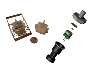
Package Design
Plastic Injection Molded
Stainless Steel & Ceramic
Hybrid, PCB, Co-fired Ceramic
Hermetic Packaging |
|
|
| Modeling and Simulation |
|
Finite Element Analysis using ANSYS™
Linear
Small Deflection
Thermal Analysis
Electrical Analysis
Non-linear
Large Deflection
Stress Stiffening
Non-linear Materials
Gap & Contact Phenomena
Hyper Elastic Phenomena
Mooney Rivlin
Blatz-Ko
Harmonic & Modal Analysis |
|
|
Electromagnetic Modeling using
ANSOFT Maxwell™
Electrostatic
Ferromagnetics
Capcitance
Inductance
Variable Reluctance |
|
|
Process Simulation using SSUPREM™
Epitaxy
Oxidation
Diffusion |
Ion Implant
Thin Films
Etching |
|
|
|